Samsung Sets up a new NAND chip plant
The new line is the largest single fabrication line in the entire industry. It took about two years of construction after breaking ground in May 2015 with a total of 15.6 trillion won worth of investment.
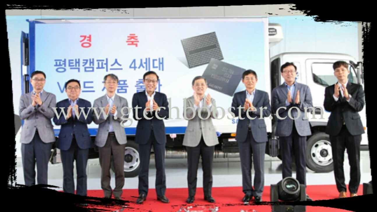
The world’s biggest memory chip provider Samsung Electronics announced Tuesday the company had officially started operation of its newest semiconductor fabrication line in Pyeongtaek, Gyeonggi Province, along with 37 trillion won ($32.2 billion) worth of investment plans by 2021. This chip plant will concentrate on the production of Samsung’s fourth-generation V-NAND (64 layers) and the first set of products will be shipped to customers soon.

The new line is the largest single fabrication line in the entire industry. It took about two years of construction after breaking ground in May 2015 with a total of 15.6 trillion won worth of investment.
Oh-Hyun Kwon, Vice Chairman and Chief Executive Officer of Samsung Electronics said
“With the dedication and support of our employees, customers, and partners, our new Pyeongtaek campus represents a new chapter in Samsung’s semiconductor operations”
Oh-Hyun Kwon, Vice Chairman and Chief Executive Officer of Samsung Electronics
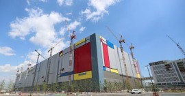
Two years after the Pyeongtaek campus broke ground in May 2015, it remains the largest single plant in the fabrication industry. There has been a sharp increase in the demand of for the next generation components basically due to the current IT trends such as Artificial Intelligence (AI), the Internet of Things (IoT), big data and automotive technologies.
Samsung, is therefore reinforcing its production abilities by investing over KRW 37 trillion in its production facilities so as to meet up with these market demands.
Samsung has a long-term plan for its manufacturing capabilities. It is believed that it will pump in a total of KRW 30 trillion into its current Pyeongtaek line to increase its semiconductor fabrication capacity. Also, detailed plans are in place for its Hwaseong, South Korea, site.
It will invest KRW 6 trillion for a semiconductor fabrication plant to boost infrastructural development which includes an Extreme Ultraviolet (EUV) equipment on the site. By 2018, Samsung Display is considering the establishment of a QLED production plant in Asan, South Korea.

Outside its hometown, South Korea, Samsung plans to construct a second semiconductor fabrication line in Xi’an. The first was constructed three years ago and it is currently in full operation. With all these investments, Samsung’s aim is to blockbuster its fabrication network worldwide.
According to Nomura Securities, Samsung Electronics will generate estimated chip sales of US$15.1 billion during the April-June period. This, if realized, will dethrone Intel from its decade-long top spot in the global chip industry.
The rosy outlook will also allow the company to report a record operating profit of 13.4 trillion won (US$11.67 billion) in the second quarter, beating Intel and Apple for the first time, according to KB Securities.
More Information
- Samsung Electronics Begins Mass Production at New Semiconductor Plant in Pyeongtaek, South Korea
- Samsung semiconductor


Gabby